
Featured

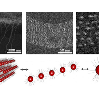
New technique simplifies creation of nanoparticle 'magic-sized clusters'
One of the cool things about nanoparticles is also what makes them so difficult to work with: the fact that their properties are dependent on their size.
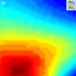
Mapping lattice strain in 4H-Silicon Carbide by synchrotron double-crystal topography
Just out in Journal of Electronic Materials is a novel strain mapping study of crystalline Silicon Carbide, a material widely used as a substrate for thin film electronics.