At CHESS, we have adopted this microfabrication technique to develop novel x-ray optics called,Collimating Channel Arrays (CCAs) [1], for confocal x-ray fluorescence microscopy (CXRF). Because the first CCA optics were fabricated from silicon substrates, the range of x-ray fluorescence energies for which they could be used, and hence the elements they could be used to study, was limited. Unwanted x-rays above about 11 keV could penetrate through the silicon, showing up as background and interfering with the measurement.
To solve the background problem, germanium substrates were used to fabricate the CCA optics. Germanium, which is much denser and therefore x-ray opaque than silicon, is also etch compatible with the fluorine etch chemistry for silicon DRIE. However, small differences in etch behavior between germanium and silicon can cause big differences in the outcome. Here, Genova et al JVST B [2] report a systematic comparison of the etch mechanisms of silicon and germanium, performed with the Plasma Therm Versaline deep silicon etcher at the Cornell NanoScale Science & Technology Facility (CNF). The etch rates of silicon and germanium were compared by varying critical parameters in the DRIE process, especially the applied power and voltage used for each of 3 steps in the etch process, on custom-designed wafers with a variety of features with systematically varying dimensions.
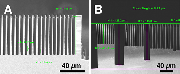
Figure 1: SEM of high aspect ratio (>13:1) etched features in Si at 3.7 μm/min (a) and Ge at 3.4 μm/min (b)
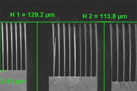
The observed etch rate for the test samples of linewidths, which ranged from tens of microns to less than 0.5µm for the same processing conditions, showed that for features with aspect ratios greater than 13:1, the etch rate of germanium is slower compared to silicon. Aspect ratios less than 13:1 on the other hand favors a faster etch rate for germanium over silicon, where the features have wider trenches. The protective polymer (C4F8), which passivates the sidewalls during the etch, was analyzed with XPS and it shows the presence of similar molecular fragments compositionally for both germanium and silicon. The germanium peaks are lower on the Ge surface by 25% compared to the Si peaks on the Si surface, suggesting that a thinner passivation polymer is formed on the sidewalls of the germanium etch. These new tricks learned from the silicon etch process are being used to fine tune a better germanium substrate etch for CCA optics.
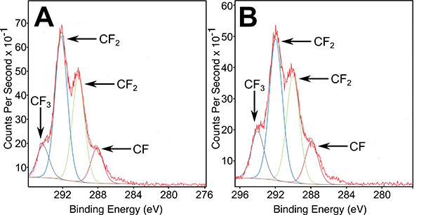
Figure 2: High resolution C1s XPS scan of molecular fragments of the passivation polymer (C4F8) deposited on the sidewall surface during a deep reactive ion etch representing the mid-trench region of Si (a) and Ge (b).
References:
[1] https://www.chess.cornell.edu/about/news/chess-technology-enables-leap-forward-trace-element-studies-archaeological-human-bone
[2] Genova, V. J., Agyeman-Budu, D. N., & Woll, A. R. Journal of Vacuum Science & Technology B, 36(1), 011205.