What is the discovery?
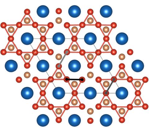
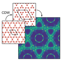
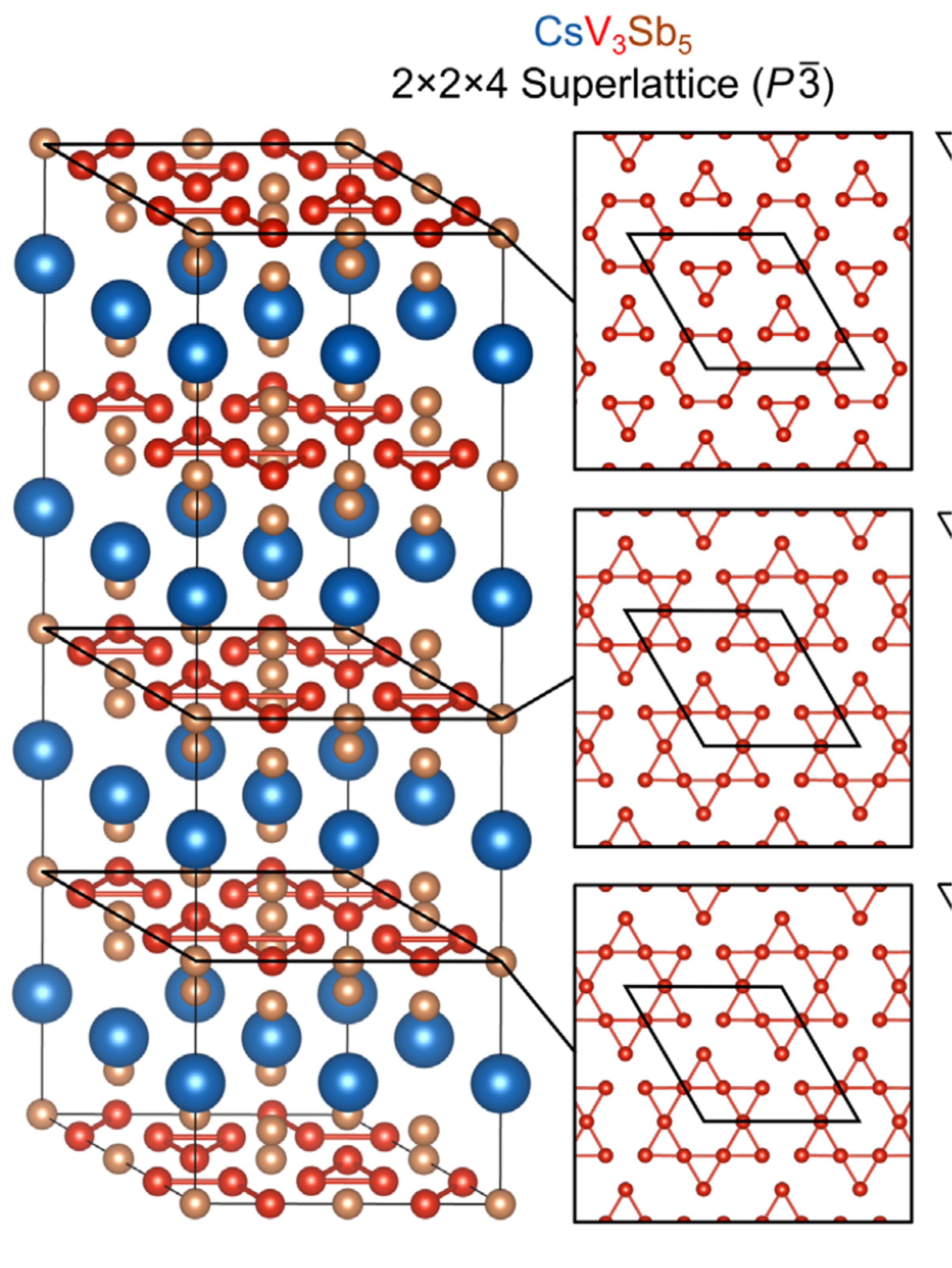
The “kagome metals” with formula AV3Sb5 (A=K,Cs,Rb) are a newly discovered family of superconducting materials. They are so-named because the positions of the vanadium atoms mimic the pattern of corner-sharing triangles in woven kagome baskets. They are of interest because they exhibit unique quantum phenomenology at low temperature, including: (i) a charge-density-wave (CDW) which may break time-reversal symmetry; and (ii) a potentially topologically nontrivial superconducting state, where widely sought quasiparticles for quantum computing may appear. In a new paper, the research group of Stephen Wilson at UCSB report a detailed study of the charge density wave phase in CsV3Sb5 and its effects on the Fermi surface. The lead authors from UCSB are Brenden Ortiz (Elings Postdoctoral Fellow) and Samuel Teicher (Quantum Foundry Grad Student Associate). Using a combination of synchrotron x-rays, quantum oscillations, and density functional theory, they demonstrate a substantial reconstruction of the Fermi surface pockets associated with the vanadium orbitals due to the CDW (Fig 1). The CDW is shown to have a correlated phasing of distortions between neighboring V3Sb5 planes, and the average structure of the CDW state is proposed (Fig 2).
Why is it important?
The kagome metals offer a brand-new playground for quantum materials research. Despite having a relatively simple and well-ordered high-temperature structure, the variety and complexity of competing quantum states at low temperatures is rich and surprising. A large community of researchers is assembling to study these effects. The goal is to understand, manipulate, and eventually exploit these new states for new quantum technologies. In order to do that, high-fidelity experimental measurements of high-quality samples are essential. Understanding the 2x2x4 CDW structure of CsV3Sb5, and understanding how it modifies the Fermi surface, are necessary ingredients for understanding the unconventional superconducting state which emerges in this material at lower temperatures.
Why did this research need CHEXS?
Detailed studies of subtle structural distortions arising from CDW phases are a core capability of the QM2 beamline at CHEXS. Identifying the 2x2x4 CDW superstructure (Fig 2) required comprehensive diffraction data, collected at low temperature and with sensitivity to weak scattering features. All this is enabled by the high-dynamic-range mapping capabilities of QM2 (high energy x-rays with helium cryocoolers, large photon-counting area detectors and very low background). The high throughput capabilities at QM2 allow for screening large numbers of crystals quickly, which is essential for researchers who are developing & discovering new materials. These capabilities anchor a successful partnership between QM2 and researchers at the Quantum Foundry at UCSB.
How was the work funded?
Q-AMASE-i: Quantum Foundry at UC Santa Barbara, NSF (DMR-1906325)
Materials Research Science and Engineering Center at UC Santa Barbara, NSF (DMR-1720256)
The California NanoSystems Institute through the Elings Fellowship program
NSF Graduate Research Fellowship Program under Grant No. DGE-1650114
The Center for High Energy X-ray Sciences (CHEXS), NSF (DMR-1829070)
The Center for Scientific Computing at UC Santa Barbara, NSF (CNS-1725797)
Reference:
Fermi Surface Mapping and the Nature of Charge-Density-Wave Order in the Kagome Superconductor CsV3Sb5
Brenden R Ortiz, Samuel ML Teicher, Linus Kautzsch, Paul M Sarte, Noah Ratcliff, John Harter, Jacob PC Ruff, Ram Seshadri, and Stephen D Wilson
Phys. Rev. X 11, 041030 ( 2021); https://doi.org/10.1103/PhysRevX.11.041030