What did the Scientists Discover?
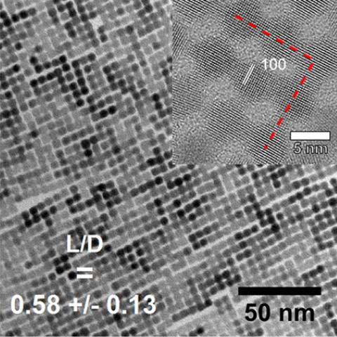
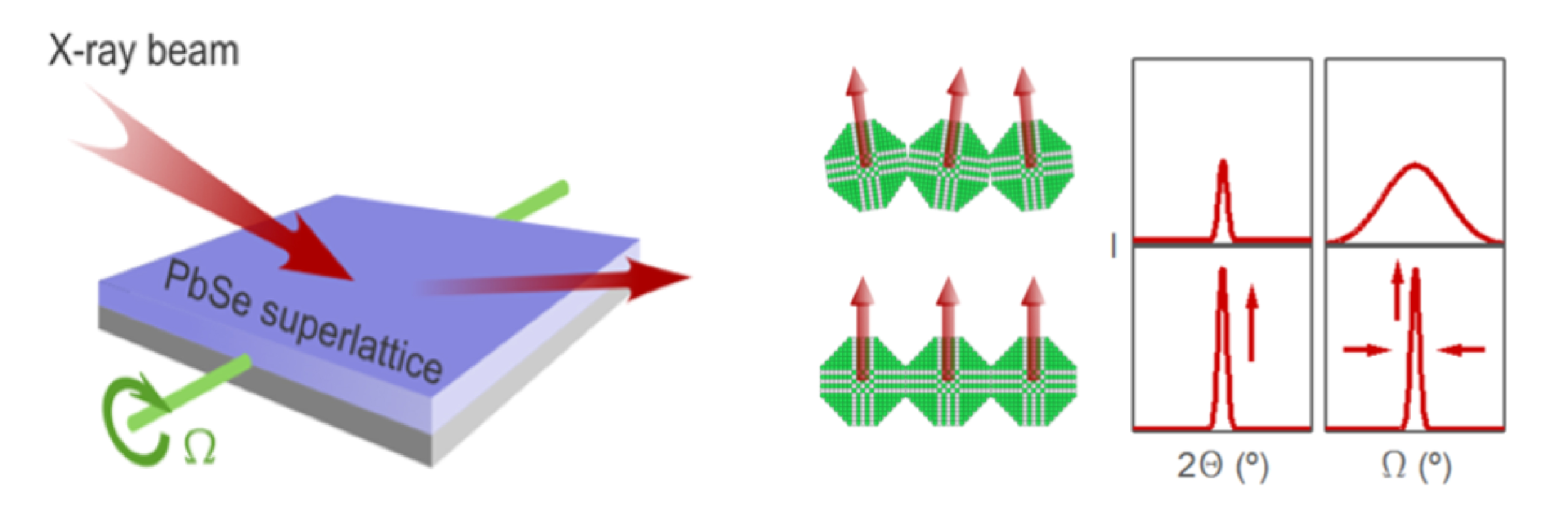
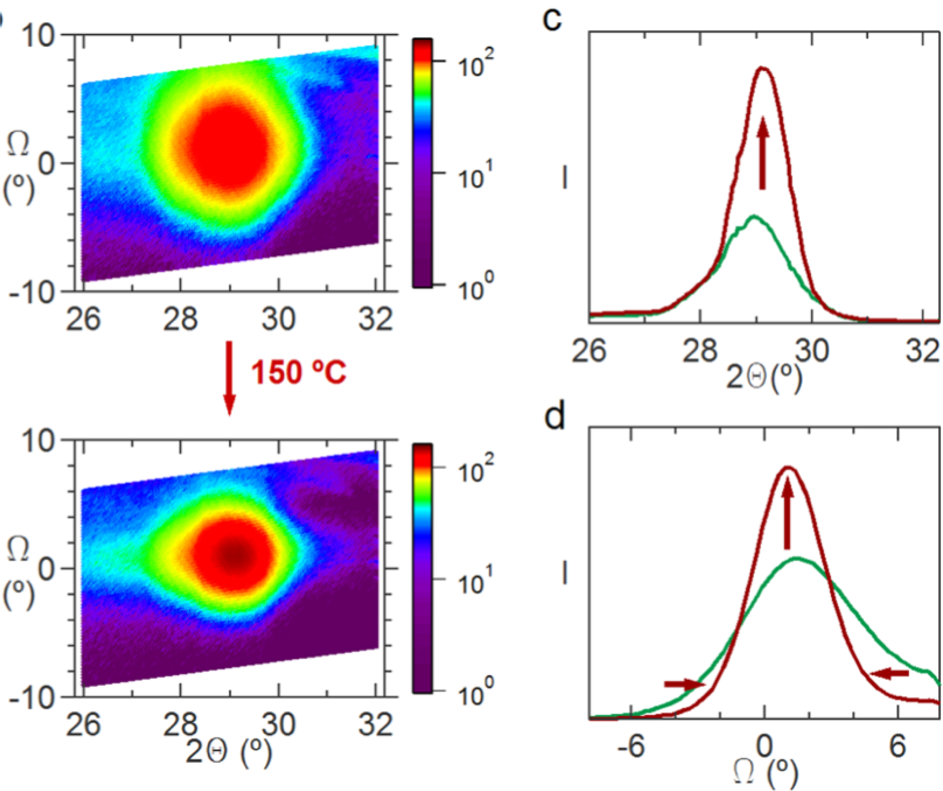
Superlattices of epitaxially connected nanocrystals (NCs) are model systems to study electronic and optical properties of NC arrays. Here, researchers show that annealing PbSe superlattices at 150oC leads to a pronounced enhancement of the charge carrier mobility and a reduction of the hopping activation energy. Since the superstructure remains intact at these annealing temperatures, X-ray diffraction studies at CHESS focused on structural disorder at the atomic scale. From rocking curve XRD measurements and a Williamson−Hall size-strain analysis, researchers find that the atomic disorder of as deposited NC arrays mainly originates from NC mosaicity, leading to edge dislocations and point defects. Through gentle annealing of the NC superlattices, both the density of edge dislocations and point defects are reduced, pointing toward the connection between defect density and optoelectronic properties of the NC superlattices.
Why is this important? What are the boarder impacts of this work?
This result indicates that the connections between NCs in as-synthesized super-lattices still form a major source of grain boundaries and defects, which prevent carrier delocalization over multiple NCs and hamper NC-to-NC transport. Over-coming the limitations imposed by interfacial defects is therefore an essential next step in the development of high-quality optoelectronic devices based on NC solids.
Why did this research need CHESS?
X-ray data for the Williamson−Hall analysis was collected at the A2 beamline at CHESS. A photon energy of 11.22 keV was used and the diffraction signal around three different reflections (002), (004), and (006) was recorded with a PILATUS detector. For each peak, the angle was tuned to the perfect Bragg condition and a single slice of the Ewald sphere was measured for one pristine and four ex situ annealed superlattices. For each film, four to five different locations on the sample were measured, and for each location the Williamson−Hall analysis conducted.
Collaborators:
- Willem Walravens, Physics and Chemistry of Nanostructures (PCN), Ghent University, Belgium
- Eduardo Solano, NCD-SWEET beamline, ALBA Synchrotron Light Source, Carrer de la Llum 2-26, Spain,
- Filip Geenen, Department of Solid State Sciences, CoCooN group, Ghent University, Belgium
- Jolien Dendooven, Department of Solid State Sciences, CoCooN group, Ghent University, Belgium
- Oleg Gorobtsov, Department of Materials Science and Engineering, Cornell University, United States
- Athmane Tadjine, Université de Lille, CNRS, France
- Nayyera Mahmoud, Photonics Research Group, Ghent University, Belgium
- Patrick Peiwen Ding, Department of Materials Science and Engineering, Cornell University, United States
- Jacob P. C. Ruff, Cornell High Energy Synchrotron Source, Cornell University, United States
- Andrej Singer, Department of Materials Science and Engineering, Cornell University, United States
- Gunther Roelkens, Photonics Research Group, Ghent University, Belgium
- Christophe Delerue, Université de Lille, CNRS, France
- Christophe Detavernier, Department of Solid State Sciences, CoCooN group, Ghent University, Belgium
- Zeger Hens, Physics and Chemistry of Nanostructures (PCN), Ghent University, Belgium
Publication Citation:
W. Walravens et al., “Setting Carriers Free: Healing Faulty Interfaces Promotes Delocalization and Transport in Nanocrystal Solids,” ACS Nano 2019, 13, 11, 12774-12786https://pubs.acs.org/doi/10.1021/acsnano.9b04757
How was the work funded?
CHESS was supported by NSF award DMR-1332208. The research was also supported by the European Commission through grants H2020-MSCA-ITN-642656, H2020-MSCA-ITN-2015-691198, HYCOAT and SBO-MIRIS; by BOF-UGent GOA nos. 01G01513 and 01G01019; by the Fund for Scientific Research Flanders (FWO-Vlaanderen); by the Semiconductor Research Corporation (SRC) Education Alliance.